
Octal D-Type Transparent Latches (3-State Outputs) Octal D-Type Transparent Latches (Inverted 3-State Outputs)
Jump to Page Section:
Overview
Description
When the latch enable input is high, the Q outputs of HD74HC373 will follow the D inputs and the Q outputs of HD74HC533 will follow the inversion of the D inputs. When the latch enable goes low, data at the D inputs will be retained at the outputs until latch enable returns high again. When a high logic level is applied to the output control input, all outputs go to a high impedance state, regardless of what signals are present at the other inputs and the state of the storage elements.
Features
- High-Speed Operation: tpd (D to Q) = 16 ns typ (CL = 50 pF)
- High Output Current: Fanout of 15 LSTTL Loads
- Wide Operating Voltage: VCC = 2 to 6 V
- Low Input Current: 1 µA max
- Low Quiescent Supply Current: ICC (static) = 4 µA max (Ta = 25°C)
Comparison
Applications
Design & Development
Models
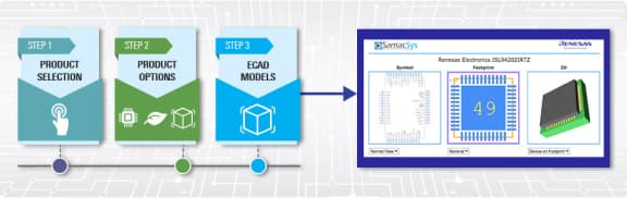
ECAD Models
Schematic symbols, PCB footprints, and 3D CAD models from SamacSys can be found by clicking on products in the Product Options table. If a symbol or model isn't available, it can be requested directly from the website.
Processing table
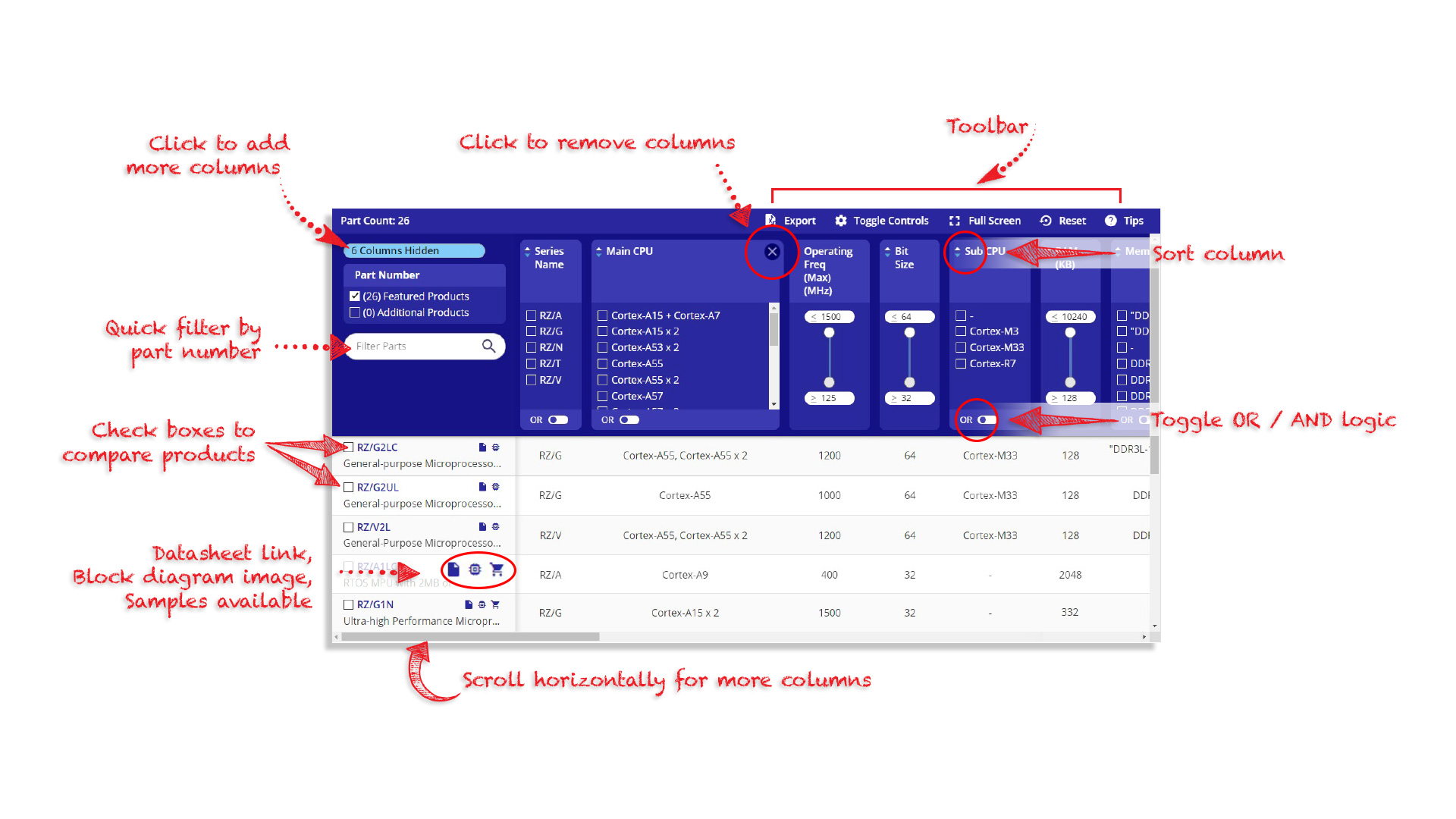
Tips for Using This Parametric Table:
- Hide Filters button in header: Collapse or expands filters
- Column sort buttons in header: Sort Column alphabetically / numerically descending or ascending
- Reset button in header: Reset all filters to the page default
- Full Screen button in header: Expand the table to full screen view (user must close out of full screen before they can interact with rest of page)
- Export button in header: Export the filtered results of the table to an Excel document
- Filter parts search bar in header: Type to filter table results by part number
- Hide column button in column headers: Select to hide columns in table
- AND / OR toggle switches in header: Toggles the logic of this particular filter to be “AND” or “OR” logic for filtering results
- Multiselect checkboxes at beginning of each row in table: Select these checkboxes to compare products against each other
- Document icon next to product name in row: View the featured document for this product
- Chip icon next to the right of the document icon in row: View the block diagram for this product
- Cart icon to the right of the chip icon: Indicates that samples are available for this product