

The semiconductor industry is going through massive advancements in digital, analog, tools, manufacturing technologies, as well as material domains. The chip development requires highly sophisticated and complex processes at all levels from design to production. Moving forward the process is going to need critical changes from architectural design to sustainable materials and end-to-end fabrication to address the growing demand for semiconductors. To achieve this, the industry is adopting the latest technologies that increase efficiency and production of highly advanced process nodes.
Semiconductors, a backbone of IoT and digital transformation:
We are witnessing significant advances in the Internet of Things (IoT), Smart devices, and more recently 5G. In order to understand where these innovations are leading us and what we should expect from them, we need to get a basic understanding of the underlying technologies that make this new wave of innovation possible. With the development of semiconductor technology driven Internet of thing (IoT) and 5G, the evolution of AI will be faster-than-ever. Semiconductor technology development has been a driving force for computing power increases in the past 30 years. It is said that semiconductors account for about 50% of the computing hardware costs. Based on semiconductor technology, the integration of AI computing devices into the society will be more seamless and pervasive. The autonomous car is an example which uses a ubiquitous constellation of mobile edge computing with sophisticated algorithms to process and analyse driving data. Based on 5G communication infrastructure, artificial intelligence (AI) and machine learning use computer vision to understand surrounding scenarios, then plan and execute safe driving movements. This makes mobility safer, smarter and more efficient. IoT devices can turn almost any product into a smart device, from watering systems to clothing. Retail, healthcare, life sciences, consumer products and industrial IoT are all in high demand.
Future innovations will also make personalized chips more accessible and make chip production more efficient and, most importantly, more sustainable. The Internet of Things (IoT) is important to the semiconductor industry as connected devices become more prevalent over time. With the smartphone industry stagnating, the semiconductor industry must find other avenues for growth potential. Despite its challenges, IoT is the most logical choice for the industry. IoT applications cannot function without sensors and integrated circuits, so semiconductors are required for all IoT devices. The smartphone market, which has driven the growth of the semiconductor industry for years, has begun to level off. The IoT market can bring new revenues to semiconductor manufacturers and keep the semiconductor industry growing at a compound annual growth rate of 3% to 4% for the foreseeable future.
Semiconductors Megatrends and Opportunities Ahead:
Semiconductor technology process nodes are the measure of the size of a chip's transistors and other components. The number of nodes has been steadily increasing over the years, resulting in a corresponding increase in computing power. Nodes often imply different circuit generations and architectures. Generally, the smaller the technology node means the smaller the feature size, producing smaller transistors which are both faster and more power-efficient. This trend has enabled us to develop more powerful computers and devices with smaller form factors. There is a relationship between process nodes and CMOS transistor performance. Frequency, power and physical size are all affected by the choice of process node. That’s why it's important to understand how semiconductor processes evolve over time. The history of semiconductor technology nodes can be traced back to the 1970s when Intel released its first microprocessor, the 4004. Since then, we have seen an exponential growth in computing power due to advances in semiconductor technology node sizes. This has enabled us to create ever-smaller and more powerful devices such as smartphones, tablets, and wearable. Apple A15 bionic today are the heart of most Apple’s latest product employs 7 nm nodes technology have almost 4 billion working transistors.
The role of process nodes in semiconductor technologies
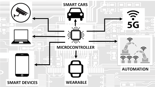
Semiconductor nodes are a key factor in determining the performance of microcontrollers. As technology advances, the number of nodes in each microcontroller is increasing. This trend has been observed over the past few years and is expected to continue in the future. A technology node (also known as a process node, process technology, or simply node) refers to a specific semiconductor manufacturing process and its design rules. Different nodes usually mean different circuit generations and architectures. Generally speaking, the smaller the technology node, the smaller the feature size, the smaller the transistor, the faster the speed, and the more energy efficient it is. Historically, process node names have referred to many different characteristics of transistors, including gate length and M1 half-pitch. More recently, the number itself has lost the exact meaning it once had due to various marketing moves and disagreements among foundries. Newer technology nodes, such as 22nm, 16nm, 14nm, and 10nm, refer only to specific generations of chips made with specific technologies. It does not correspond to gate length or half-pitch. Nonetheless, the naming convention is respected, which is what the leading foundries call the nodes.

Early semiconductor processes had arbitrary names, for example, HMOS III, CHMOS V. Later, each new generation process is called a technology node or process node, expressing the gate length in terms of the minimum feature size of the nanometer (or historically 1 micron) process of the process transistor, such as "90 nm process". However, things have changed since 1994 and the number of nanometers used to name process nodes has become a marketing term that has nothing to do with actual feature size or transistor density (number of transistors per squared) mm).
The evolution of technology node process
Essentially, technology node corresponds to the physical feature size of the transistor. Originally, every microcontroller is built out of transistors, which are basically switches which control the flow of electric current and allow the microcontroller to perform its logical function. Technology nodes such as 28 nm or 65 nm are referring to the minimum data graphic feature which can be drawn on the layout (half pitch or gate length). However, there is no standardisation in naming of technology nodes. The name of a node such as 28 nm or 65 nm is actually coming from the minimum gate length of the transistor as shown in the conventional planar MOSFET configuration. Generally, technology nodes give an indication of how densely transistors can be packed per millimeter square substrate. Starting from 22 nm technology, the technology has switched to fin field effect transistor (FinFET) where the architecture behind FinFET is in three-dimensional configuration and the term of gate length is no longer fit to describe the process technology. Nowadays, technology nodes such as 10 nm and 5 nm do not correspond to any gate length or half pitch distance anymore as the technology switched from planar structure to FinFET or Gate-all-around FET (GAA FET).

Renesas is playing a vital role in new process technology development to enable next-generation IoT devices. With the Internet of Things (IoT) becoming more prominent, device designers are now looking for ways to make their devices smaller, faster, and more energy efficient. To meet these demands, Renesas has developed a new process technology that enables IoT devices to be significantly smaller than before while using less power. The 40nm process is optimized for Flash-based microcontrollers with lowest power consumption and highest performance in mind, whereby the 110nm is optimized for wide voltage range and lowest power operation. The result is for example RL78, RA or RX microcontrollers from Renesas that can perform faster than ever before and consume less power than ever before while still retaining all of its functionality and features.
Renesas has been a leading provider of semiconductor solutions for industry and consumer electronics, and also known for its advanced work in developing new technologies to support the Internet of Things (IoT) and more recently in AIOT (Artificial Internet Of Things). One example of this is our focus on developing in-house low power process technology in the area of 110nm, known as MF4. It allows Renesas to develop super low-power consumption devices applicable for a wide range of endpoints. The demand for such low-power devices has become increasingly important as we move toward in a world where everything from our cars to our appliances are connected to the internet and as more devices come online, demand for energy consumption increases. In order to address this issue, Renesas has developed a new power management system that reduces energy consumption by up to 30%. This new system allows them to build smaller chips that require less power than ever before.
The extensive microcontroller and SOC product lines from Renesas offer a wide range of digital and analog functionalities including wide performance ranges and low power consumption or energy harvesting capabilities, required for diverse IoT applications. To support your design from beginning to end, Renesas also offers partner platforms, software, and development tools. Renesas' ICs and modules enable you to precisely perceive, comprehend, and send intelligent data from sensor to cloud. You are invited to take advantage of our advanced semiconductor technologies that address your power, performance, and security requirements and enable you to offer next-generation design in record time.