概览
简介
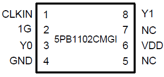
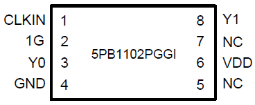
The 5PB1102 is a high-performance 1:2 LVCMOS clock buffer. It has best-in-class Additive Phase Jitter of 50fsec RMS.
The 5PB1102 also supports an Output Enable function. It is available in 8-pin DFN and TSSOP packages and can operate from a 1.8V to 3.3V supply.

特性
- High performance 1:2 LVCMOS clock buffer
- Very low pin-to-pin skew <50ps
- Very low additive jitter <50fs
- Supply voltage: 1.8V to 3.3V
- fmax = 200MHz
- Integrated serial termination for 50ohm channel
- Packaged in 8-pin TSSOP and small DFN packages
- Extended (-40°C to +105°C) temperature range
产品对比
应用
设计和开发
模型
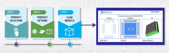
ECAD 模块
Schematic symbols, PCB footprints, and 3D CAD models from SamacSys can be found by clicking on products in the Product Options table. If a symbol or model isn't available, it can be requested directly from the website.
Processing table
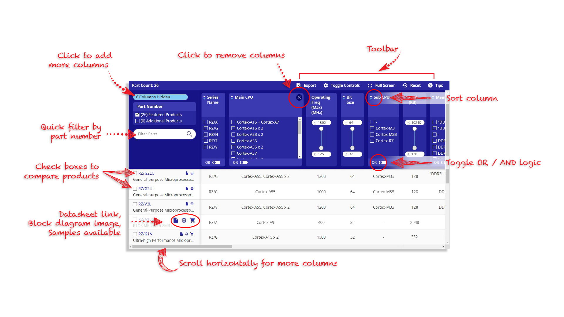
Tips for Using This Parametric Table:
- Hide Filters button in header: Collapse or expands filters
- Column sort buttons in header: Sort Column alphabetically / numerically descending or ascending
- Reset button in header: Reset all filters to the page default
- Full Screen button in header: Expand the table to full screen view (user must close out of full screen before they can interact with rest of page)
- Export button in header: Export the filtered results of the table to an Excel document
- Filter parts search bar in header: Type to filter table results by part number
- Hide column button in column headers: Select to hide columns in table
- AND / OR toggle switches in header: Toggles the logic of this particular filter to be “AND” or “OR” logic for filtering results
- Multiselect checkboxes at beginning of each row in table: Select these checkboxes to compare products against each other
- Document icon next to product name in row: View the featured document for this product
- Chip icon next to the right of the document icon in row: View the block diagram for this product
- Cart icon to the right of the chip icon: Indicates that samples are available for this product
视频和培训
5PB11xx Ultra Low Jitter LVCMOS Buffers
This video provides an overview of the LVCMOS High Performance Clock Buffer Family, highlighting their key features and capabilities.

Video List
新闻和博客
| 博客 | 2018年12月15日 | ||
| IDT Introduces Ultra-Low-Jitter Family of LVCMOS Clock Buffers | 新闻 | 2015年3月30日 |