
High-speed Circuit Technologies and Silicon Measurement Results of MCU Test Chip Presented in ISSCC 2024
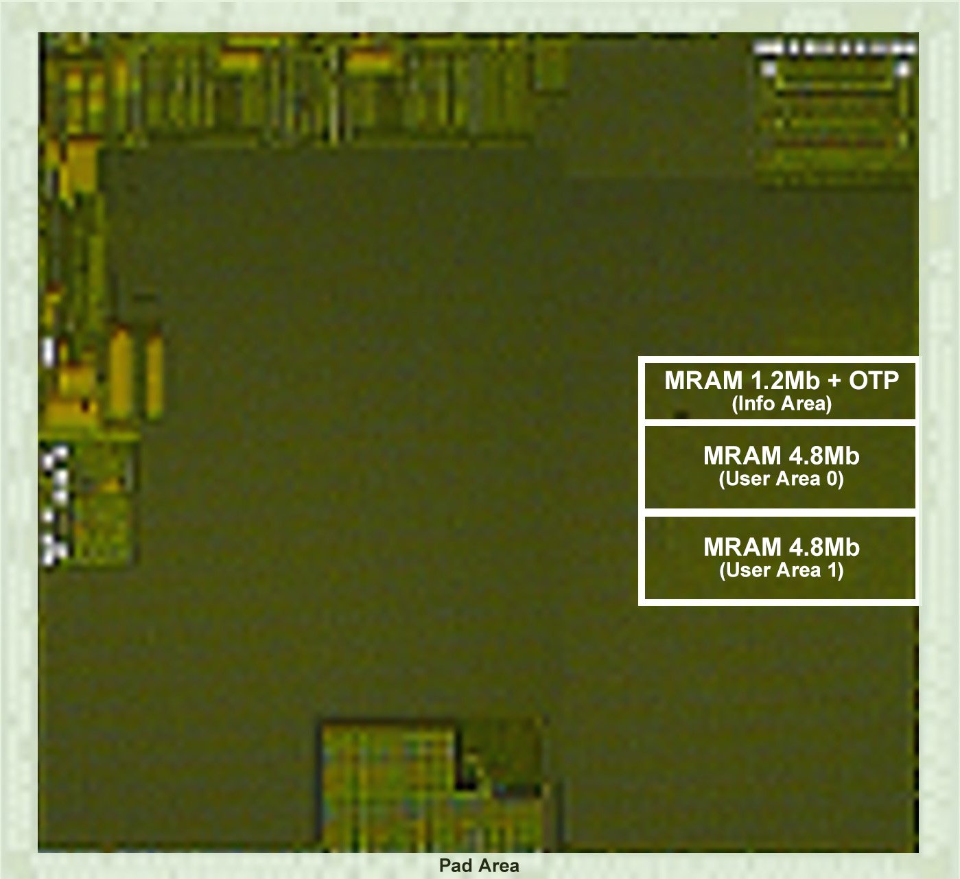 Embedded STT-MRAM Test Chip
TOKYO, Japan ― Renesas Electronics Corporation (TSE:6723), a premier supplier of advanced semiconductor solutions, today announced that it has developed circuit technologies for an embedded spin-transfer torque magnetoresistive random-access memory (STT-MRAM, hereinafter MRAM) test chip with fast read and write operations. Fabricated using a 22-nm process, the microcontroller unit (MCU) test chip includes a 10.8-megabit (Mbit) embedded MRAM memory cell array. It achieves a random read access frequency of over 200 MHz and a write throughput of 10.4-megabytes-per-second (MB/s).
Renesas presented these achievements on February 20 at the International Solid-StateCircuits Conference2024 (ISSCC 2024), held between February 18 and 22, 2024, in San Francisco.
As IoT and AI technologies continue to advance, MCUs used in endpoint devices are expected to deliver higher performance than ever. The CPU clock frequencies of high performance MCUs are in the hundreds of MHz, so to achieve greater performance, read speeds of embedded non-volatile memory need to be increased to minimize the gap between them and CPU clock frequencies. MRAM has a smaller read margin than the flash memory used in conventional MCUs, making high speed read operation more difficult. On the other hand, for write performance, MRAM is faster than flash memory because it requires no erase operation before performing write operations. However, shortening write times is desirable not only for everyday use, but also for cost reduction of writing test patterns in test processes and writing control codes by end product manufacturers.
To address these challenges, Renesas has developed the following new circuit technologies to achieve faster read and write operations in MRAM.
(1) Fast Read Technology
MRAM reading is generally performed by a differential amplifier (sense amplifier) to determine which of the memory cell current or the reference current is larger. However, because the difference in memory cell currents between the 0 and 1 states (the read window) is smaller for MRAM than for flash memory, the reference current must be precisely positioned in the center of the read window for faster reading. The newly developed technology introduces two mechanisms. The first mechanism aligns the reference current in the center of the window according to the actual current distribution of the memory cells for each chip measured during the test process. The other mechanism reduces the offset of the sense amplifier. With these adjustments, faster read speed is achieved.
Furthermore, in conventional configurations, there is large parasitic capacitance in the circuits used to control the voltage of the bitline so it does not rise too high during read operations. This slows the reading process, so a Cascode connection scheme (Note 1) is introduced in this circuit to reduce parasitic capacitance and speed up reading.
Thanks to these advances, Renesas can achieve the world’s fastest random read access time of 4.2 ns. Even taking into consideration the setup time of the interface circuit that receives the MRAM output data, we can realize the random read operation at frequencies in excess of 200 MHz.
(2) Fast Write Technology
For the write operation, the high-speed write technologies for embedded STT-MRAM announced in December 2021 improved write throughput by first applying write voltage simultaneously to all bits in a write unit using a relatively low write voltage generated from the external voltage (IO power) of the MCU chip through a step-down circuit, and then used a higher write voltage only for the remaining few bits that could not be written. This time, Renesas takes into account that because the power supply conditions used in test processes and by end product manufacturers are stable, the lower voltage limit of the external voltage can be relaxed. Thus, by setting the higher step-down voltage from the external voltage to be applied to all bits in the first phase, write throughput can be improved 1.8-fold.
Combining the above new technologies, a prototype MCU test chip with a 10.8Mbit MRAM memory cell array was fabricated usinga 22 nm embedded MRAM process. Evaluation of the prototype chip confirmed that it achieved a random read access frequency of over 200 MHz and a write throughput of 10.4 MB/s at a maximum junction temperature of 125°C.
The test chip also contains 0.3 Mbit of OTP (Note 2) that uses MRAM memory cell breakdown to prevent falsification of data. This memory can be used to store security information. Writing to OTP requires a higher voltage than writing to MRAM, making it more difficult to perform writing in the field, where power supply voltages are often less stable. However, by suppressing parasitic resistance within the memory cell array, this new technology also makes writing in the field possible.
Renesas continues to develop technologies for embedding MRAM in MCUs (IEDM 2021, VLSI 2022). These new technologieshave the potential to dramatically boost memory access speed to over 200 MHz, enabling higher-performance MCUswith embeddedMRAM. Faster write speed will contribute to more efficient code writing to endpoint devices. Renesas is committed to further increasing the capacity, speed, and power efficiency of MRAM.
Notes
- Cascode connection is a configuration to connect a common source transistor in series to a transistor with a DC gate bias applied.
- One-Time-Programmable memory. Configuring a part of the MRAM memory array to be converted to OTP makes it possible to implement an OTP with a smaller area than a general OTP macro that uses eFuses or oxide film breakdown of transistors.
About Renesas Electronics Corporation
Renesas Electronics Corporation (TSE: 6723) empowers a safer, smarter and more sustainable future where technology helps make our lives easier. The leading global provider of microcontrollers, Renesas combines our expertise in embedded processing, analog, power and connectivity to deliver complete semiconductor solutions. These Winning Combinations accelerate time to market for automotive, industrial, infrastructure and IoT applications, enabling billions of connected, intelligent devices that enhance the way people work and live. Learn more at renesas.com. Follow us on LinkedIn, Facebook, X, YouTube, and Instagram.
(Remarks) All names of products or services mentioned in this press release are trademarks or registered trademarks of their respective owners.
The content in the press release, including, but not limited to, product prices and specifications, is based on the information as of the date indicated on the document, but may be subject to change without prior notice.